The symbols are unveiled, the axioms condense.
Saturday night ..designing a quantum mechanical adder circuit using balanced logic gates EI (either) and AND.
The symbols for the balanced form of logic gates are directly correlated to their graphical expression upon a four quadrant graph. Over the center-point and origin of the graph are plotted two diagonal vectors that neatly form an X shape.
For each of the two vectors there exists an appropriate and obvious symbol.
EI (either) = \ (backslash, EI) ..(-1,+1) (+1,-1)
AND = / (forwardslash, AND) ..(-1,-1) (+1,+1)
The first consideration beyond the logical function is the physical circuit design of Qbit architecture chosen by DWave.
These logic gates can therefore be represented as an addressing and argument statement. One which should address the two Qbits of a logic gate along with the quantum mechanical coupling between them.
No transistors here...
We needed no less than ten transistors (XOR + AND) to build a half-adder.
Using a system of Qbits and couplings that allow control of quantum superposition and the shared state of entanglement...
..EI and AND will need to be expressed in terms of the minimum two channels required for a decision structure such as a logic gate.
..the declaration of quantum coupling states expresses the functions of exception (EI) along with inclusion (AND).
The DWave instruction set does include argument (coupling) based control of Qbit spin states. The coupling allows the spin states of two Qbits to be matched/parallel ..the coupling also allows the complementary opposing spin state in relation to the coupled Qbit (+1, -1) (1, 0).
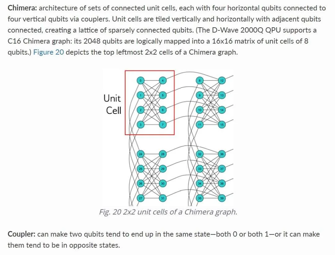
Considering the Chimera architecture diagram, at fist glance it seems complicated beyond comprehension. There is a way to simplify and accurately express the relationship between a single Qbit among the others in this specific architecture.
..one vertex of a two dimensional shape will always be the intersection of two sides, three dimensional shapes produce a vertex that intersects with three sides.
Now when we consider the Chimera architecture, we can understand that each Qbit is a vertex coupled to five other Qbits by five individual couplings (sides). Each Qbit can now be logically considered one vertex of a five dimensional object.
We do not need five dimensions ..for the moment. It will suffice to first surmount the obstacle of addition by means of balanced logic gates implemented using the quantum mechanical effects of superposition and entanglement logical correlations (perpendicular/same couplings).
Wait... (perpendicular/same couplings)... (perpendicular/same couplings, EI/AND).......
..we are interfaced, quantum logic to mechanics. The logic and function seem fitted for the tasks.
Now, to build a circuit that can perform a binary addition...
Okay, so no matter how many dimensions (sides) intersect with a vertex ..we have a simple mapping that can represent our balanced EI and AND statements ..EVEN in the event of an architectural change to more or less dimensions, the EI and AND logic gates should still be applicable.
What is interesting, how we might build our circuits to take advantage of these couplings which replace incredible and very real numbers of components required to express classical computing logic (DC, transistors) for performing work such as addition.
A Coupling in the context of bitwise operation = Order of magnitude, bit specific operations for binary operation handling.
For an eight Qbit binary number, we need eight couplings (8 sides to 8 vertices). A Qbit operation for each successive order of magnitude (10110011, eight binary digits).
Base 2 to the power of N-digits... eight couplings for N-digits and eight Qbits to store the values zero and one for each order of magnitude among the eight (base two) digits.
I realize the quantum processor is not currently intended for such an application, really this is a quantum leap over the transistorized version ..the component reduction is staggering and the timing ..??? ..wow.
It would be convenient to represent the action of Qbits as parallel streams of data in the form of square waves for the intensities +1, 0 (superposition) and -1. Of course -1, +1 need to be handled as 0, 1 for binary terms and operations.
For three lanes, two are recording Qbit function while the middle lane records the changes in the state of the coupler. Coupler state changes represent the EI (either) and AND balanced logic gates. One connection to the coupler and one for Qbit state read.
For data accuracy, more couplers and qbits can be allocated to simultaneous error correction of our "virtually infallible" eight Qbit quantum byte.
In the case of best 2/3 matching answers, simultaneous error correction for one byte requires an extra two couplers with two Qbits for the error correction. For 2/3 simultaneous error correction, our Qbyte will require 3 * 8 = 24 Qbits and 3 * 8 = 24 Couplers.
24 Qbits and 24 couplers for one eight Qbit 2/3 error corrected Qbyte.
Hi-Precision can be implemented using a three matching of five (3/5) simultaneous iterations for error correction.
3/5 error corrected Qbit structure:
40 Qbits and 40 Couplers for one eight Qbit 3/5 Hi-Precision error corrected Qbyte.
YES!!!! ..success.
5 vertices and 5 sides for each simultaneously error corrected Qbit of one Qbyte. A perfect-fit five dimensional implementation of a 3/5 error corrected Qbyte using ALL of the five dimensions available to each vertex (Qbit) of the Chimera architecture.
Hi-Precision error corrected quantum computing presents the possibility of operating the superconducting chips above the current temperatures which are 100X colder than interstellar space. Such an error corrected process can bring quantum computing outside of it's purely scientific environment. While limiting the operational speeds to a fraction of a full Q by means of the error correction, necessary for the chip to operate reliably with less interference protection or temperatures that can be reached using cost-effective instrumentation. Out of the lab into farms then homes.
I believe this configuration to yield a fixed direction, yet is a compromise considerate of all parties involved.
We have organized our error corrected Qbits in the form of a long contiguous binary datapath. Across a 2000 Qbit QPU we can potentially map 660 Qbits (error corrected 2/3). With Hi-Precision 3/5 error correction, 400 Qbits.
Need an eight bit byte? ..32 bits? ..512 bits? ..660 bits? ..the instruction set can allocate values to as many or as few bits as necessary, for operations and caching ..handled by the instruction set, on behalf of higher level programs.
Base 2 to the power of 660 binary bits = the maximum binary number in one process.
This configuration can allow the porting of software to and from classical computing as a bridge to the quantum computing processor. Along with the appropriate instruction sets, the QPU is equipped to produce operating environments that match software from other platforms.
Some organizations may very well like to be computing the same old things with the advantages of QPU quantum mechanics.
So much has been considered, no binary addition yet.
The interesting part is that quantum mechanics has made complex transistor based decision structures obsolete. The majority of those physical circuits now exist in far fewer components.
Decision structures and operations now belong entirely within the instruction set. There are less points of failure if we do not consider the interferences to which quantum mechanical processors are susceptible.
To add one to a binary number or carry to the next digit (order of magnitude) a coupler can be addressed to apply each bitwise operation. The method of adding will rely on evaluation before wasteful bit changes are applied, a potentially more efficient method than add and carry.
It can remember more predefined rules than a human, the quantum computer will not be required to add then carry-over as humans do while performing addition. Changes the bit value in current digit to 0 while changing the value in the next digit by 1 using the appropriate couplings.
I consider this binary addition...
SOLVED :)
..next challenge, the DWave instruction set implementation.